In the era of ultra-high-definition display, LED packaging technology keeps pace with the times
Release Time:
2022-05-17 17:09
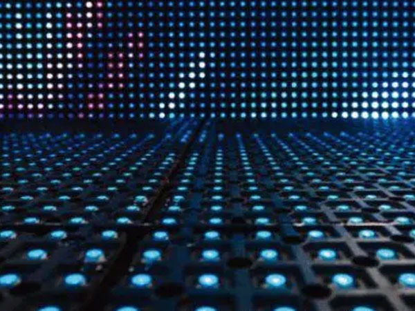
As people continue to pursue the ultimate visual experience, the demand for ultra-high-definition displays is increasing day by day, and LED displays have entered the era of micro-pitch. The LED display has developed from the past single-color to two-color, and then to full-color; the dot pitch is also shrinking, from the previous P30 to P20, P10, P2.5, and then to the LED display below P1. Rapid development.
Under this trend, LED packaging technology has also continued to improve and develop in the direction of diversification.
The arrival of ultra-high-definition display, N-in-1 SMD came into being
Regarding the production of red (R), green (G), and blue (B) primary color chips in color science, it has been developing continuously as early as 20 years ago, and the packaging methods of chips have also become diversified, from DIP packaging to today. SMD, COB package, etc.
SMD surface mount package
When the LED display screen moves from the outdoor to the indoor, the chip size continues to develop to the micron level with the shrinking process. The SMD surface packaging device is applied to the indoor display screen and has matured. The corresponding LED chip size is 3535, 2121 et al.
Driven by the high-definition pixel drive of indoor LED small-pitch displays, the size of LED chips has developed from 2121 down to 1515 and 1010. LED displays with a dot pitch of P1.2-P2.5mm are not very different, and there is a phenomenon of homogeneous competition.
With the advent of the 5G+4K/8K+AI era, the market increasingly needs ultra-high-definition LED displays below P1. At this time, the size of LED chips below P1 develops downward to 0808 and 0606, and the packaging structure design faces challenges in process and production yield, thus resulting in the concept of N-in-1 SMD.
CCTV takes the lead in promoting the development of "5G+4K/8K+AI"
For example, the four-in-one SMD uses a space of 1.5mm in length and width to divide four areas, and package four red, green and blue chips at one time. The N-in-1 SMD has the opportunity to achieve a MiniLED display with a smaller dot pitch without changing the surface-mount manufacturing mode.
N-in-1 SMD package
SMD surface mount applications have certain limitations in small-pitch displays, such as electrostatic effects, bumps during handling and installation, which are easy to damage lamp beads, etc., and the protection level is relatively weak.
GOB and AOB enhance protection functions and improve stability and reliability
Aiming at the limitations of SMD packaging technology, there are mainly two solutions in the industry, GOB and AOB. By surface treatment on the light board module, it can play the role of moisture-proof, dust-proof and anti-static, and avoid bumps and scratches. The problem of lamp bead damage occurs, which provides a strong guarantee for the stability and reliability of ultra-high-definition display.
Waterproof, dustproof, antistatic function
Among them, GOB technology is a surface coating process, similar to the surface gluing process of outdoor display screens. A layer of transparent epoxy resin is filled on the surface of the SMD lamp board as a whole, and the surface of the lamp bead is covered with a thickness of 2~5mm, which can prevent dust. and waterproof effect.
GOB technology is suitable for LED displays with large spacing, such as P8 and P10. If it is applied to LED displays with small spacing, it is not easy to dissipate heat, resulting in excessively high temperature on the surface of the display and blurring of the optical display effect.
AOB technology
AOB is a nano-level surface coating coating process, which mainly includes a filling layer and a surface protection layer. The filling layer improves the ink color of the printed circuit board and the optical effect of the lamp surface, so that it can achieve a wide viewing angle and is suitable for small-pitch LED displays; the surface protective layer prevents the lamp bead pins from being intruded by water vapor and dust. The application of AOB technology takes AET Qingyun series as a typical case.
Latest News
2022-05-17
LED packaging structure, process development status and trend
LED packaging is a technology involving multiple disciplines (such as optics, thermals, mechanics, electricity, mechanics, materials, semiconductors, etc.). (As shown in Figure 1) From a certain point of view, LED packaging is not only a manufacturing technology (Technology), but also a basic science (Science), excellent packaging engineers need to understand thermal, optical, material and process mechanics Have a deep understanding of the nature of physics.
Read More →2022-05-17
From chip to package to terminal, interpret the development status of UVC LED
In the past two years, affected by the global economic downturn and geopolitical conflicts, the growth rate of the global LED lighting market has slowed down significantly.
Read More →2022-05-17
LED packaging form and packaging process
LED chip types are mainly divided into three categories from a structural point of view: horizontal electrode chips, flip chips and vertical electrode chips.
Read More →Tel: +86-519-89806999
Fax: 86-519-86523668
Address: No.98 Wunan Middle Road ,Wujin, Changzhou,Jiangsu ,China
E-mail: amicc@amicc.com
Web: http://www.amicc.com
SupplierIn Quiries →
Copyright © 2022 Jiangsu AMICC Optoelectronics Technology Co., Ltd. Powered by www.300.cn 苏ICP备*********号-1


